KiCad for PC is an open-source electronic design automation (EDA) software suite used for creating schematics, printed circuit board (PCB) layouts, and structural electronic designs. Initially developed in 1992 by Jean-Pierre Charras, the application has evolved into one of the most popular tools for electronics hobbyists, engineers, and professionals alike.
Its robust feature set combined with its open-source nature makes it a highly versatile choice for PCB design, fully capable of handling both small-scale hobby projects and complex, multi-layer industrial designs.
Overview and Key Features
-
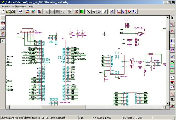
Schematic Capture (Eeschema): Create complex circuit schematics utilizing an extensive library of components and custom symbols. Supports hierarchical sheet designs for managing large-scale projects.
-
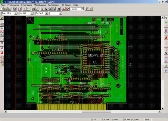
Professional PCB Layout (PCBNew): High-performance board design module supporting multi-layer boards, differential pair routing, and high-speed layouts. Features an interactive routing tool with real-time Design Rule Checking (DRC) to ensure manufacturability.
-
Integrated 3D Viewer: Features a built-in 3D visualization engine that allows users to inspect the physical layout, verify component clearance, and view the populated PCB in a three-dimensional space prior to manufacturing.
-
Extensive Library Management: Comprehensive built-in libraries for components, footprints, and symbols. Includes full capabilities for creating, importing, and managing custom user libraries.
-
SPICE Circuit Simulation: Integrates natively with Ngspice for advanced circuit simulation, enabling users to test, analyze, and verify electrical functionality before physical prototyping.
-
Modular Interface: Divided into specialized modules (Eeschema, PCBNew, etc.) within a unified project manager. Supports multiple windows, tabs, and customizable hotkeys for an optimized workflow.
How to Use
-
Launch the application and select New Project to establish a dedicated directory for your project files.
-
Open the Eeschema module to construct your circuit schematic by placing components from the library and connecting them with wires.
-
Assign physical footprints to each schematic component.
-
Switch to the PCBNew module, import the netlist from your schematic, and arrange the component footprints on the board canvas.
-
Utilize the track routing tools to connect the components according to design rules.
-
Open the 3D Viewer from the top menu to visually inspect the physical component placement and board layout.
-
Generate and export Gerber files, drill files, and bill of materials (BOM) needed for commercial PCB manufacturing.
Pros and Cons Pros
-
Completely free and open-source with no licensing costs or subscription fees.
-
No board size, layer count, or component limitations on any project.
-
Highly active community with frequent updates and vast shared footprint libraries.
-
Advanced interactive router allows efficient high-speed design and trace length tuning.
-
Cross-platform compatibility across Windows, macOS, and Linux. Cons
-
Steeper learning curve for users migrating from commercial software like Altium or EAGLE.
-
Library configuration and custom footprint creation can be complex for beginners.
-
UI structure is split into independent modules rather than a single fluid workspace.
Top Alternatives
-
Altium Designer: Industry-standard, premium commercial EDA software tailored for advanced enterprise PCB design.
-
Autodesk EAGLE: Popular PCB design and schematic software featuring robust cloud integration and fusion capabilities.
-
EasyEDA: A web-based, user-friendly EDA tool suite tightly integrated with component catalogs and manufacturing services.
-
Fritzing: An open-source, beginner-friendly prototyping tool designed for hobbyists to document hardware layouts easily.